
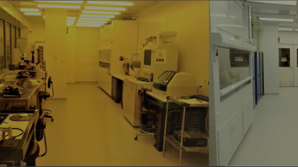
The School of Engineering (SoE) Nanofabrication Core Facility offers measurement instrumentation, wet processes and majority of process tools for a range of research activities. The core objectives of the Facility include supporting research activities of Rutgers School of Engineering, educating students and postdocs with skills and capabilities that can be readily applied in high-tech semiconductor industries and research institutes, promoting research collaborations between research centers and industrial organizations, bringing in Research Incomes through Grants, User Access Fee and Trainings and leading the applications of federal and state-funded competitive fundings.
Key Resources
- Fabrication Tools: Atomic Layer Deposition, Ebeam #1, Ebeam #2, MOCVD, PECVD_Plasma Therm, PECVD_Unaxis, Reactive Ion Etch, Reactive Ion Etch, Rapid Thermal Anneal, Sputter_Denton-DV502, Sputter_Sys & Des Fab, Sputter_Denton, Furnace_Boron, Furnace_Phosphorus, Furnace_Oxidation, Furnace_Anneal/FGA, Plasma Treatment_Barrel Etcher, UVozone Cleaner, Dicing Saw_Disco, Dicing Saw_K&S, Laser Scribing, Marking and Ablation (Innotech), Thermal Evaporator (Logitek), Wafer Spin Rinse Dryer, Photoresist Spinner (Laurel), Mask Aligner (Karl-Suss MJB3)
- Wet Chemical Process: Silicon Etch (HF:HNO3), Silicon Etch (TMAH), Silicon Surface Texturing (TMAH), Caro Etch (H2SO4:H2O2), Aluminum Etch (H4PO4:HNO3:CH3COOH), RCA Clean (NH3:H2O2:H2O, HCL:H2O2:H2O), Palladium Etch (CH3COOH:HNO3:HCL), Boiling HNO3 for oxide growth, Buffered Oxide Etch, Silver Etch (HNO3), Oxide/Nitride Etch (HF fume)
- Characterization Tools:Detek Non-Contact Profilometer, 4-Point-Probe (Ossila), Film Metric, Optical Microscope, UV & Solar Simulator, Scanning Electron Microscope
Location
New Brunswick/Piscataway
Contact Name
Ngwe Zin
Contact Email
ngwe.zin@rutgers.edu